Get the errata (mistakes) for the textbook.
| General Information: |
| Title: | ECE/CS 5710/6710 - Digital VLSI Design - Fall 2016 |
| Instructor: | Ken Stevens, kstevens@ece.utah.edu, MEB 4506, 801-585-9176 |
| Classes: | Tue & Thu 5:15pm - 6:35pm, WEB 2230 |
| Office Hours: | by appointment |
| Web Page: | www.eng.utah.edu/~kstevens/5710/ |
| TA: | James Skowronek and Derek Moore, teach-5710@list.eng.utah.edu |
| TA Hours: | Cade Lab: T,H 3pm-8pm (James) T,H 3:30-5pm (Derek) W 12-2pm (Derek), W 3-5p (James) |
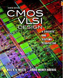
| Text Book 1: | Principles of CMOS VLSI Design: A Circuits and Systems Perspective By Weste & Harris |
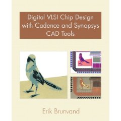
| Text Book 2: | Digital VLSI Chip Design with Cadence and Synopsys CAD Tools, By Erik Brunvand. |
| Prerequisites: | ECE/CS 3700, Verilog or VHDL |
| Course Description: |
This is the introductory course in VLSI where you will learn how to drive Electronic Design Automation (EDA) Computer-Aided Design (CAD) tools. With them you will learn the physical mask design for transistors and how to create and characterize your own logic cell library. You will then use your cell library to design a complete integrated circuit architecture including power delivery and bonding pads.
Many aspects of Digital VLSI design will be introduced in order to take this significant and enjoyable design journey. However, note that this is not a course in digital system design or computer architecture. You will already need to know Verilog, boolean logic, and how to design and implement combinational and sequential digital circuits (such as adders and other datapath logic, and finite state machines). The project will also require some knowledge of computer architecture for you to complete a moderately large digital design. We recommend you take ECE/CS 3810 (Computer Architecture) before this course.
Topics that will be covered in lectures include:
The class will require extensive use of CAD tools. All of the CAD tools required will be available in the CADE lab. Students must have an account that will allow them to use the CADE machines. These tools do not run on MS Windoze. Therefore some familiarity with various versions of Unix (such as Linux or Solaris) and the X window system is required for this course.
The tools will be discussed in class and you will receive the aid of the TA in the labs and project. However, there is no specific lab class that you are required to attend. You can perform the labs and your project at your own convenience, either in the CADE lab at the University, or across the network. Remember that nothing can replace taking the time to read the CAD tool documentation.
Integrated circuit design is mastered only through experience, so this is a hands-on course with lots of labs and project time. The homework, as well as lectures, will be closely tied to the term project, the design of a simple standard cell library and then the use of that library to design a project. The final library and project will be done in teams (preferably made up of 3 to 4 students). The initial design of cells for the project will be done individually. You must complete the design of these cells on time. You are encouraged to interact with others, but until you are asked to form teams, the work on your cell designs, simulations, etc., must be independent and fully your own work.
Fabrication of your final project is possible thanks to the research funding provided through the MOSIS service. Few tasks are more rewarding than creating a functional integrated circuit. However, few tasks are also more disappointing that spending time on the design of an integrated circuit only to have the fabricated circuit return non-functional. Therefore, careful design practices must be followed if you are to fabricate your chip including sufficient Design-For-Test, validation of your design, and a quality design review. If you do fabricate the chip, you will be required to take ECE/CS 6712 in the spring to test and report on the results.
 |
Principles of CMOS VLSI Design: A Circuits and Systems
Perspective (4th Edition), By Neil Weste and David Harris.
Published by Addison-Wesley, c2011, ISBN 0-321-54774-8. Get the errata (mistakes) for the textbook. |
 |
Digital VLSI Chip Design with Cadence and Synopsys CAD
Tools, by Erik Brunvand. Published by Addison-Wesley, c2010
ISBN 0321547993 Note: The there is an update for the book to map from the version 5 to version 6 of the Cadence design tool interfaces. You will need to use this in conjunction with the book to efficiently use the tools. |
Logic Effort - designing fast CMOS Circuits, I. Sutherland, B. Sproull, and D. Harris. Academic Press, 1999
Analysis and Design of Digital Integrated Circuits (3rd ed), David Hodges. McGraw Hill, 2004.
The Design and Analysis of VLSI Circuits, Glasser and Doberpuhl. Addison-Wesley, 1985.
There are two class mailing lists, 5710@list.eng.utah.edu and teach-5710@list.eng.utah.edu. The 5710 list will be used to send out important information to everyone in the class. Please use discretion when sending messages to the entire class. Mail sent to teach-5710 just goes to the instructor and TA. This is the preferred method of communicating with the TA and instructor.
The lists will be automatically populated with your university mailing address. If you would like to add another e-mail address, you can send a subscribe request by logging on to the UofU sympa mailing list server. Let me know if you would like to remove your university e-mail address in lieu of another preferred address.
| Grading Policy: |
Refer to the College of Engineering Guidelines for more detail on appeals, disabilities, adding, and withdrawing from courses.
| Incomplete Policy: | You can't get an incomplete unless you have a documented medical or legal emergency. |
| Add/Drop Policy: | The standard University Policy is applied. |
| Disability: | If you have a condition that merits consideration, you must contact the instructor at the beginning of the course. |
| Labs and Homework | 40% |
| Final Design Review | 5% |
| Mid-term Exam: | 15% |
| Project (design and report) | 40% |
The homework will take the form of problem sets, project proposals, and other written work. The Labs will involve using the VLSI CAD tools to design the mask work and layout of cells that will be used in your project. The class project will require the design of a small digital standard cell library that will then be used as a cell library for a moderate sized functional design. Class members will then join into design teams for the implementation of the design. The design review will consist of a short presentation of the project to the class. The project report will be a paper in conference or journal format.
Those taking the graduate level course will have additional requirements that include a more rigorous project or design flow and the review of one or more papers relating to VLSI from journals or conferences in the area. These could be related to the project being implemented.
Details on the requirements for your project reports. Please refer to my links for 6712 and 6770 for example reports students have delivered in previous years.
| Homework Assignments: |
The labs and homework build upon each other during class.
These need to be completed on-time!
There is no general provision for late work.
Please read this document on design requirements that will greatly improve your productivity and ability to complete the lab assignments on time!
Labs must be tar'ed up and turned in via canvas.
The labs and assignments are listed here when given:
| Date Due | Description |
| Sept 2nd | Review Quiz This graded quiz will help you brush up on your basic skills, and is due in class. Must be completed independently by each student. |
| Sept 9th | Lab 1 Schematic capture and Verilog simulation. Reading: Design with Cadence & Synopsys, Chapters 1 - 4. |
| Sept 23rd | Lab 2 Layout editing, DRC, LVS, SPICE simulation. Reading: Design with Cadence & Synopsys, Chapters 5 - 7. |
| Oct 2nd | Lab 3 Flip-Flop and register design. Reading: Design with Cadence & Synopsys, Chapters 3 - 6. Reading: Principles of CMOS VLSI Design, Chapters 1 & 10. |
| Oct 9th | Assignment: Form groups for future labs and project (e-mail to teach) |
| Oct 20th | Lab 4 Transistor operation, DC simulation. Reading: Design with Cadence & Synopsys, Chapter 7. Reading: Principles of CMOS VLSI Design, Chapter 1, 2 & 4. |
| Oct 30th | Lab 5 Five cell library. This is a group lab! Reading: Design with Cadence & Synopsys, Chapters 8 & 9. |
| Nov 6th | Midterm Exam |
| Nov 10th | Lab 6 Cell characterization, additional library cells (group lab). Reading: Design with Cadence & Synopsys, Chapters 8 - 10. |
| Nov 11th | Team Project Proposal Turn in a pdf file on canvas by start of class. Refer to the project reporting requirements |
| Nov 20th | Lab 7 Cell drive strengths, Place & route, and CPU synthesis (group lab). Reading: Design with Cadence & Synopsys, Chapter 11. Reading: Principles of CMOS VLSI Design, Chapters 3 - 5. This is the last lab! |
| Dec 9,11th | Team Project Presentation in class
|
| Dec 12,15th | Schedule Design Review with Instructor and TA
|
| Dec 17th | Completed Design Due Paper Review Due (6710 Section Students) Team Member Peer Evaluation Due Final Team Project Report Due |
| approx. Jan 16th | Design and GDS Stream Due for chips to be fabbed
|
| Lecture Notes: |
 Introduction to VLSI and transistors
 Introduction to Layout
 Introduction to writing Test Benches
 Physical design and Layout
 MOS Transistor Theory
 IC Fabrication
 Logical Effort
 Verilog as a Synthesis Language
 Overview of Lab 5
 Synthesis and Place & Route
 Library Footprints
 Simple MIPS Processor Design
 Simulation Choices
 Hierarchical Block Assembly
 Pads and Chip Fabrication
| Team Assignments: |
Think about with whom you would like to do your final project. We will form teams by October 2nd.
Following are the team assignments for team lab assignments and class meetings and presentations.
| Useful Links: |
 Crafting a Chip:
A practical guide to the UofU VLSI CAD Flow, by Erik
Brunvand.
 Project Ideas
for your team.
 Information on the
CAD tools installed at the University of Utah.
 Circuits & Layout Lecture
notes by Prof. David Harris.
 Scalable CMOS Design Rules document.
 The
First Chapter of Sutherland, Sproull, and Harris' book on Logical Effort.
 Logical Effort Lecture
notes by Prof. David Harris.
 Here are several Verilog guides to help you brush up on your coding.
This includes a single page reference sheet,
a quick reference guide,
and a simulation focused handbook
(although I have philosophical reasons that this is the wrong
use for a synthesis language...).
 Verilog coding styles for IC design is provided by Synopsys covering
general mistakes such as with latch interference,
if and case statements,
if and case statements for late arriving signals,
for logic building blocks,
and high performance designs.
 The
VGA mini-project that you will want to look at if you will be
building a design driving VGA graphic displays.
 Additional information on
VGA timing.
 If you want memory in your project you should use the
single and dual ported SRAM generator
library developed at Utah.
 If you want to use ROM cells in your project, use the
ROM tutorial based on a past student's code.
You can also see his documentation on makemem,
but be warned that this currently only functions for ROMs, and not RAM.