Ken Stevens
Associate Professor
University of Utah
Electrical and Computer Engineering
Salt Lake City UT
e-mail: kstevens@ece.utah.edu
The Post Office Project
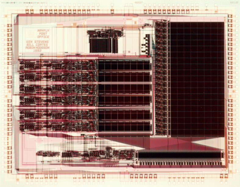
The Post Office is the communication coprocessor developed by Ken Stevens
at Hewlett-Packard as part of the Mayfly project. The Mayfly architecture
is a general purpose parallel processor, often called a distributed
ensemble architecture. Multiple processing elements (or PEs )
cooperate to solve single complex problems which have been broken into
smaller parallel computations. There is no globally shared memory. Task
spawning and communication between processes on different PEs are carried
out via message passing. The Post Office chip is the communication
coprocessor which supports this internode message passing.
Performance was critical to the success of the full-custom CMOS VLSI Post
Office chip begun in 1987. The complete chip was the largest and most
complex fully asynchronous integrated circuit in published work when
fabricated. It consists of approximately 300,000 transistors with an
external bandwidth of 2.5 Gigabits per second and PE interface bandwidth of
1 Gigibit per second. There are seven complete ALUs for routing
calculations. The part scales up to a distributed processor containing a
maximum of 519,841 PEs (limited by the size of the address word).
Final silicon was fabricated in 1992 and tested in 1993. Ken Stevens
designed the network, routing algorithm, and Post Office architecture, as
well as the state machines, circuitry, and full-custom layout with the
exception of the RAM cells and drivers that were implemented by Bill
Coates. Robin Hodgson did much of the integrated testing of the Post
Office in a 7 element Mayfly prototype.
The Post Office was fabricated through the MOSIS service on an HP 1.2
micron CMOS process and has an area of 11 X 8.3 mm. The control portion
consists of 95 different asynchronous finite state machines, most of which
operate concurrently and occupy 19% of the chip area. Datapath circuitry
accounts for 45%, pads cover 11%, wire routing occupies 22% of the chip
area, and the remaining 3% of the space is unused on the rectangular 84 pin
die.
The Post Office effort was challenging and interesting for several reasons:
- It was a pioneering coprocessor for distributed ensemble
routing architectures. Its design preceded CalTech's wormhole routing
and multi-queue architectures.
- The design is massively parallel, with a complex control structure.
- The Post Office is an asynchronous chip placed into a
synchronous environment.
- It was the most complex fully asynchronous single integrated circuit
in published work.
- It was built in a commercial environment where performance
was an important aspect.
Additional Features of the Post Office
-
 Scalability.
The scalability of the Mayfly architecture is probably the single most
important argument in favor of an asynchronous Post Office design. The
physical extent of the Mayfly architecture is formally unbounded, and the
size of an implementation is only limited by the size of the address word.
The current Post Office chip supports instantiations of up to 519,841
PEs. The ability to arbitrarily scale the architecture poses serious
technical problems if a global clock is necessary to synchronize
operations. Clock skew can be a problem in itself for synchronous design as
technology progresses. For extensible systems such as the Mayfly where the
PE count is unbounded, synchronizing all of the nodes with a single clock
becomes intractable.
- Robustness.
The robustness of functional, asynchronous interfaces removes the
problems of clock skew and simplifies link arbitration and transfer
synchronization. Mayfly processors are composed by simply plugging
the Post Office links together (subject to topological constraints).
Each PE in the multiprocessor contains a local crystal and a clock
generator that runs at its own clock speed. Processor speeds for
communication between PEs are irrelevant due to the asynchronous
interface. One PE in the HP prototype running at an internal clock
speed of 16 MHz communicates perfectly well with another running at
64 MHz via the Post Office chips.
- Low Power.
The low power nature of asynchronous architectures was one further
advantage demonstrated in the Post Office. Asynchronous circuits contain
fine grain, dynamic power management due to the handshake protocols. Each
idle Mayfly PE requires 30 amperes of current at 5 volts. By way of
contrast, the Post Office, which is the only asynchronous part in the
system, uses only 2 milliamps when idle. (Accurate active power numbers
were not compiled.)
Interesting Spinoffs
The complexity, low latency requirements, and inherent parallelism of the
Post Office made the current asynchronous design styles impractical. While
single input change (or SIC ) techniques were well developed,
they were not directly applicable to Post Office control due to the amount
of parallelism present. When several inputs to a SIC asynchronous finite
state machine ( AFSM ) may change simultaneously, they must be
filtered or combined with input conditioning which makes the design more
difficult, and area and performance suffer. Some MIC techniques overly
restricted the arrival time of signals. The stored state model I used
previously for integrated circuits was a fairly unrestricted multiple input
change (or MIC ) model, but its implementations were also very
large and the response time was slow. Other MIC methods required inertial
delays (delays that can filter out small duty cycle transitions) or delays
on the feedback lines which were also unsuitable for performance oriented
designs.
My solution for implementing low latency state machines designed for
parallel process forking and synchronization was to invent the burst-mode
hazard model. Performance was further improved by transforming
sum-of-products descriptions into complex gate CMOS
implementations. Burst-mode permits a restricted form of MIC signaling
which supports hazard free sequential logic and simplifies the
implementation of hazard-free combinational logic in asynchronous finite
state machines. It also results in small, intuitive specifications.
During the implementation phases of the Post Office project it became
evident that automated synthesis tools are a necessary and viable
alternative to hand generation of hazard-free AFSM logic. A burst-mode
synthesis tool called MEAT was developed by
Coates, Al Davis, and myself to aid in the design of the Post Office. MEAT
was used in the development of 90% of the control modules in the Post
Office. MEAT produced circuit designs comparable in area and performance
to the hand designs. Dave Dill's verifier was ported to the burst-mode
hazard model developed for the post office implementation by Steve Nowick.
This further aided in the AFSM design as it contributed to the removal of
all hazards under burst-mode in a majority of the leaf cells. The utility
of MEAT and the verifier resulted in a larger portion of the effort to be
directed toward the layout and simulation of the chip, two additional areas
that can be supported by software tools.
The need for a stronger means of assuring correct system behavior became
apparent after the first silicon was fabricated and a deadlock was
discovered. Simulation techniques proved ineffective and inefficient in
discovering the cause of the deadlock, motivating a stronger formalism for
validating system behavior. Although formal methods cannot detect all the
failures (such as the dynamic logic error) in the Post Office, the need to
make stronger assertions about the properties of a large parallel circuit
was a great motivator for the development of
Analyze . These tools are a step towards the production of an
asynchronous workbench capable of the practical synthesis and verification
of asynchronous circuits.
The design effort of the Post Office also influenced fresh work by others
in a number of areas. Some of these contributions include:
- Burst-mode is becoming widely used as a hazard model for the
synthesis and formal verification of asynchronous AFSM implementation.
- Design vignettes of the Post Office are available to the asynchronous
community for tool benchmarking and design challenges, including a set of
Post Office state machine specifications, novel CMOS device implementations
such as the SEQUENCER, and design problems such as the nonblocking arbiter.
- Other design and synthesis projects have been spawned as a
direct result of the Post Office work. This includes research done at the
HP science center at Stanford University, and the thesis work on AFSM
synthesis by Nowick and Ken Yun.
- Improved algorithms and methods for hazard-free design have
been developed by Nowick as a result of this project.