Assignment 4
Assignment
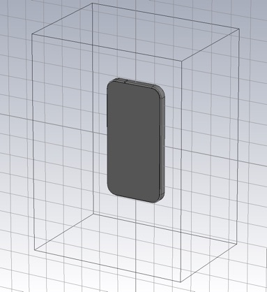
We will simulate something vaguely resembling an iPhone 4 antenna and determine its properties with and without a finger on the, so called, “death spot”.
First construct a model that captures the basic configuration of the handset’s antenna. It is possible that (as this person believes) the antennas are essentially slot antennas as outlined in an Apple patent.
Start a new project, without using a project template. Set up our usual units (mm, GHz, nS). Set the frequency range to 0 to 2 GHz. Set the Background Material to Normal with Epsilon = Mue = 1.
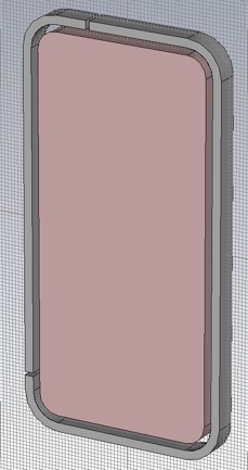
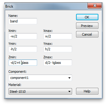
The innards (between the glass front and back) can be modeled as a single brick of metal. The outer-most part will be a steel band circumscribing the handset with two splits to create slot antenna boundaries. Use Copper (annealed) (lossy) for the innards and Steel-1010 (lossy) for the outer band, though obviously these are rough approximations. Use global parameters for all the geometric properties so we will have ample tuning capability. Use blend radii that lead to uniform cross-sections in the outer band and the slot.
Use global parameters and formulas to specify the geometry. For example:
For initial values use:
exterior corner radius = 10mm
lateral exterior dimensions use Apple tech specs
metal thickness = 6.3 mm
glass thickness = 1.5 mm
outer band width = 2.5 mm
slot width = 2 mm
left lower slit position, below center = 43 mm
left upper slit position, left of center = 10 mm
split width = 1 mm
Now add the glass to the front and back. Use Glass (Pyrex) (lossy) because we do not have a model for the fancy aluminosilcate glass that Mr. Jobs specified.
Set the glass back from the edge as on the real handset. For an initial value of the set back use 1 mm, and again, use blending radii such that all blends have the same center of curvature.
Set all boundaries to open (add space), since we want the antennas to radiate into an infinite space and we will not need to de-embed any waveguide ports. You may want to see where the simulation domain Bounding Box is. You can set this to be visible by checking Bounding Box in the View Tab.
Since our model of the handset is mirror symmetric, front-to-back, you can add one symmetry plane, for a 2X speed-up. Electric or magnetic? This symmetry plane must be compatible with the fields generated by the discrete port. Another way to think about it is to consider what would happen if you put zero impedance surface or a zero admittance surface at the proposed location.
Now add a discrete ports that will function as an antenna feed. Use the default 50 Ohms for the impedance (a guess). The Discrete Edge Port panel is accessible from the Simulation Tab.
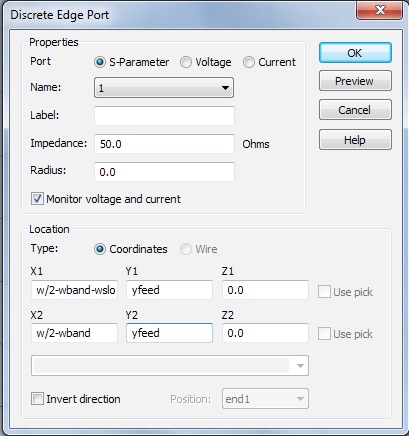
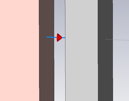
When selected the port is shown as a blue line with a red cone indicating the polarity. It should span the slot, and should probably lie in the center (front to back) of the slot. For the initial value of the vertical posiiton of the feed, choose 40mm below the center. You probably want to zoom in and hide the glass to confirm the port is where it ought to be.
Now we can simulate. We will use the optimizer to find locations of the splits and feed that will maximize the antenna efficiency. For the purpose of seeing the optimizer progress in a reasonable amount of time, we will prioritize speed over accuracy. Open the Time Domain Solver Parameters panel. Leave the accuracy at -30dB. Under Specials... , increase the Number of pulses to a bigger number like 200, and give the frequency samples a modest boost to 4001 from 1001.
Now select Optimizer...
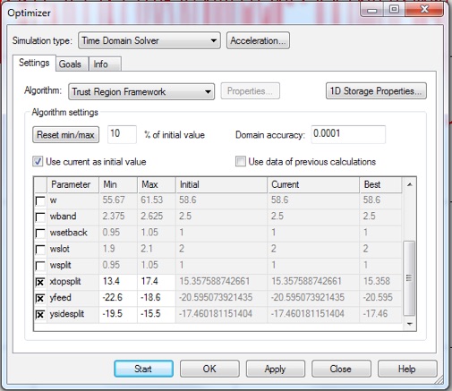
In the Parameter table select the variables controlling the locations of the feed and the splits, and give them the biggest range that keeps the splits and feed on the straight portion of the band. Select one of the global optimization algorithms. I used the Genetic Algorithm.
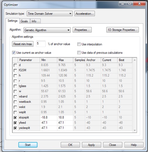
Click OK.
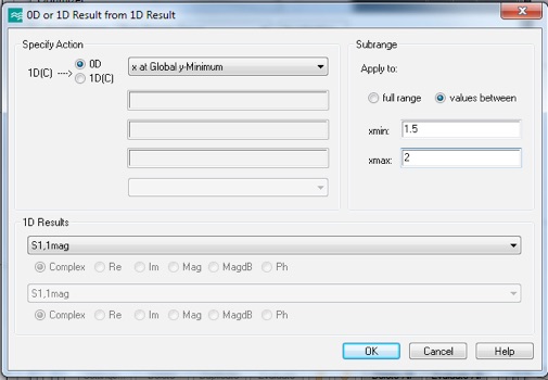
Select 1D Result from 1D Result in the bottom menu again. This time pick Global y-Minimum. Use the same subrange.
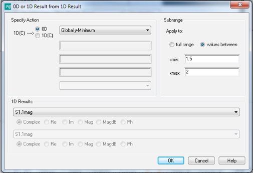
Click OK. Then close the Template Based Postprocessing panel.
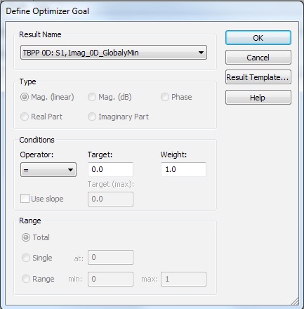
In the Define Optimizer Goal panel, select xAtGlobalYMin, and use the = operator, a variable for the Target, and 10 for the weight.
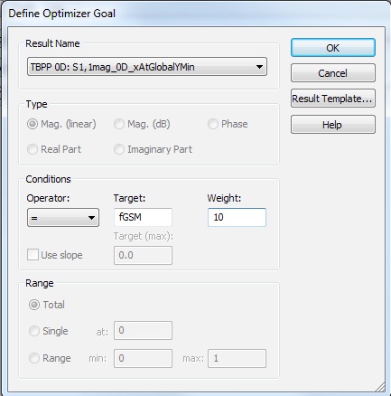
Click OK. Our frequency target will be a GSM band. Specifically, the middle of the
DCS-1800 Uplink band. http://en.wikipedia.org/wiki/GSM_frequency_bands
Add another goal for GlobalyMin.
Now click Start to begin the optimization. Each sim should take about 15 to 60 seconds. Let it run until you get a Sum of all goals less than 0.5,
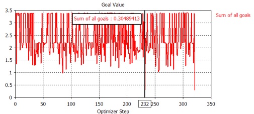
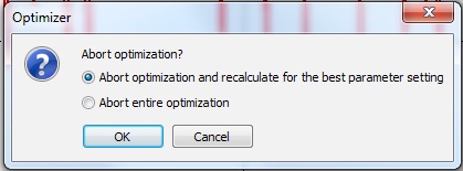
Now abort, and choose recalculate.
The best parameters will be displayed in the Optimizer Info tab, and with greater precision, in the Parameter List. Record these values with a screen grab, in case something goes wrong.
Now, starting from these globally optimized parameters, use a local optimizing algorithm. For this, we want to optimize the actual efficiency (instead of just minimizing S11), so we need to create a far-field monitor. From the Simulation tab, select Field Monitor. Choose Farfield/RCS, and enter a variable for the Frequency.
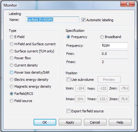
For the frequency we will use the center of DCS-1800 Uplink band. To see the goals associated with this field monitor in the optimizer, you need to run a simulation and get results for the monitor. Run a single simulation. Now, open the optimizer, and add a new goal. Choose Efficiencies/linear/Tot. Effic. [1] from the menu. Select the = operator and a target of 1.
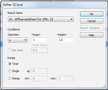
You may want to clear the Tables before starting this new optimization. Use Delete Results in the Post Processing tab. You will have to close the Optimizer panel to do this.
Start the optimizer. You should manage to reach a total efficiency of at least 0.75. If you are having trouble reaching this goal, get help from me.
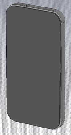
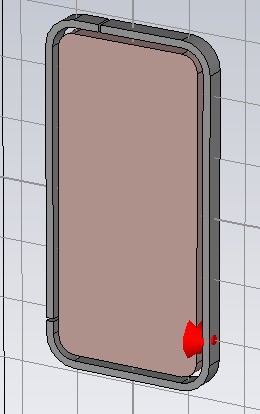
1. Provide a picture of the phone in the optimal configuration (with the glass hidden), and report the numerical positions of the splits and feed with respect to the handset center.
-
2.For the optimal configuration, report the fractional power distribution of the stimulated power, specifically report the fractional power: reflected, radiated and absorbed. The absorbed power is whatever is left over from reflection and radiation, and will include power absorbed in the copper, steel, and glass.

Of the absorbed power, what fraction was absorbed in the copper steel, and glass.

Now let us try to simulate the death grip. Get the electromagnetic properties of wet skin from this excellent website. In particular get the conductivity and the relative permittivity of wet skin at our operating frequency. (We will assume these properties are relatively constant over the GSM band.) Make a new material with these properties.
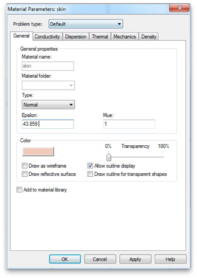
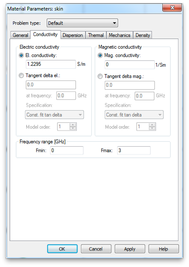
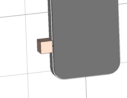
Put a cubic centimeter of this material centered on, and touching, the left-side split. Re-simulate.
-
3.Report the power distribution as in question 2. What is the drop in radiated power (in dB) induced by touching the split? Where is most of the power going, that is now not being radiated? Did the absorbed power go up or down? Why?
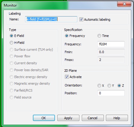
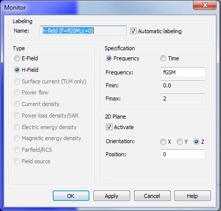
Let’s add some local field monitors for both E and H. In particular, we want to look at our operating frequency and in the plane of the slot.
Make sure your far field monitor is still present, and run one last simulation at the optimal configuration.
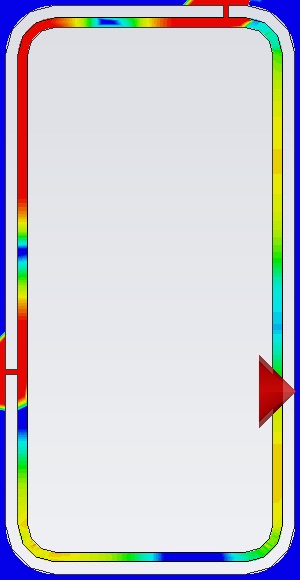
4. Include the following E and H plots of the slot fields in your report. Select from the navigation tree: 2D/3D Results>>E-field>>e-field (f=fGSM,z=0)>>Abs. Then from the 2D/3D Plot tab click Properties and then Plot amplitude from the Phase/Animation selections. Back in the 2D/3D Plot tab, you can adjust the Clamp to Range values to best display the field minima and maxima of the fields in the slot.
Do the same for the H-field.
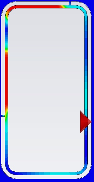
Consider the magnitude of both E and H, and identify positions of maximum and minimum characteristic impedance of the slot waveguide. Mark these locations on either your E or H plot (or both), with a ‘+’ and ‘-’ for maxima and minima respectively. Is the feed point closer to an impedance minima or maxima? What is the approximate impedance at the location of the feed? Is the impedance a maximum or minimum at the splits? What does this suggest is the termination condition of the slot waveguide at the splits.?
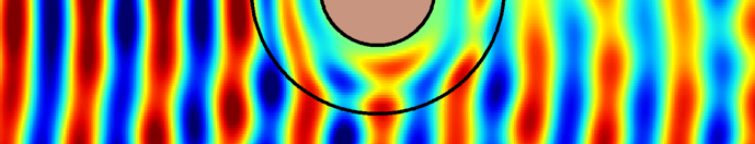
5. Include a far-field plot in your report. Select from the navigation tree: Farfields>>farfield (f=fGSM). From the Farfield Plot Properties, make the phone appear together with the radiation pattern. Include a couple views that communicate most of the pattern geometry.
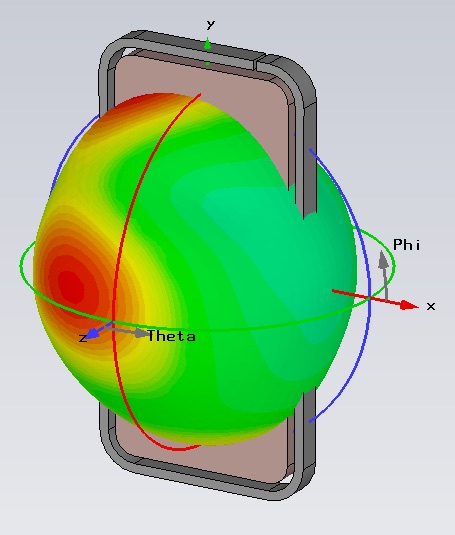
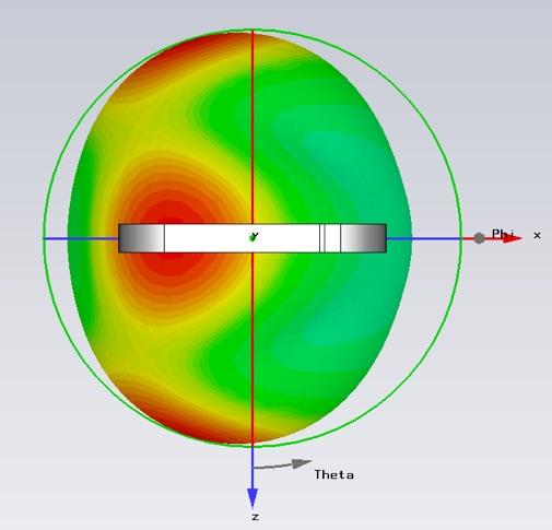
Describe two qualitative differences in the radiation pattern between this antenna and a dipole antenna. How does this antenna’s directivity compare to that of a half-wave dipole antenna? How does the longest dimension of this phone compare to the length of a half-wave dipole at our operating frequency?