
Assignment 1
Balanis Problems
1.9, 1.27, 1.45, 2.6, 2.20
CST Problem: Faraday’s Law
Open CST Studio Suite from the Start menu and double click the CST Microwave Studio icon in the upper left.
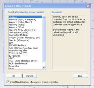
Accept the template <None> by clicking OK.
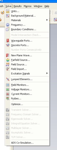
Generally, to construct a simulation you work your way down the Solve menu. Select Units...
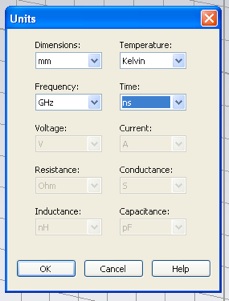
Select the units mm, GHz and ns, which will be convenient for this problem.
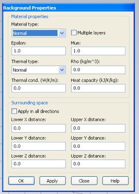
Now select Background Material... from the Solve menu and choose Material Type Normal. Leave the Epsilon and Mue values at 1.0, that is vacuum.
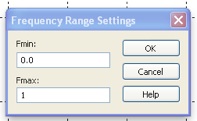
Now select “Frequency...” from the Solve menu and set the maximum frequency to 1 GHz.
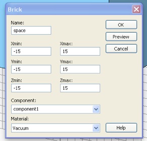
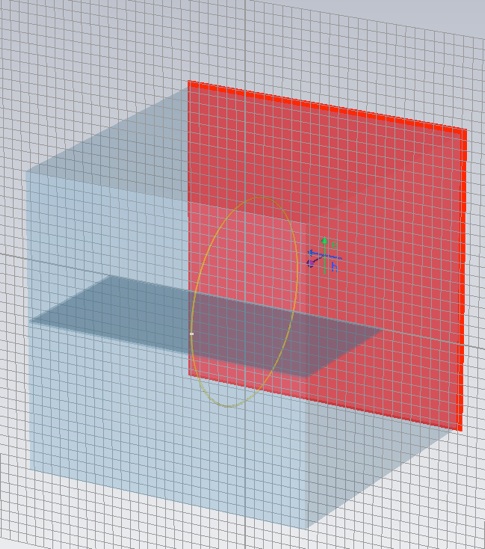
Now we start populating our simulation domain with material objects. We start with a block of vacuum. Click the brick creation icon (a small cube).
Press the esc key to bring up the numerical entry panel. Make a cube of Material Vacuum with side dimensions 30 mm, centered on the origin. (I named it space.)
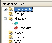
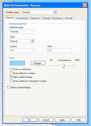
I like to make the Vacuum material more transparent. You can do this by double clicking Vacuum in the materials folder of the Navigation Tree.
This will bring up Material Parameters panel for Vacuum. Adjust the Transparency slider to taste.
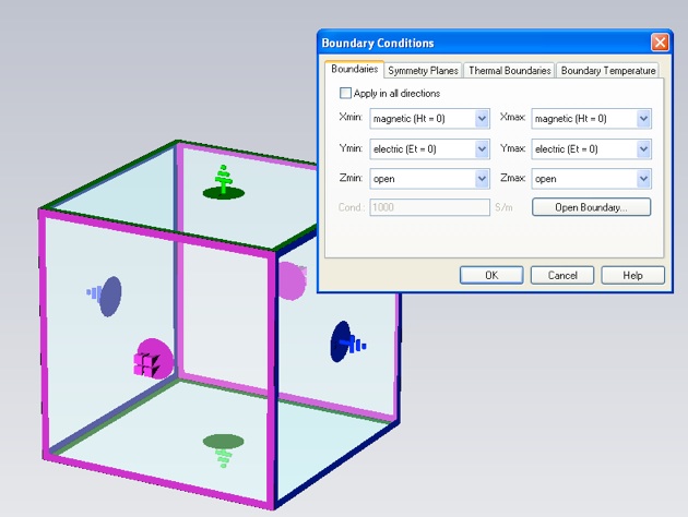
Next select Boundary Conditions... from the Solve menu. Set the boundary conditions as shown. (The graphical view will only show all the boundary conditions, as below, after you have closed (clicked OK) and reopened the panel.) These boundary conditions are compatible with sending in a plane wave along the z-direction with the electric field polarized in the y-direction. Importantly, the magnetic field of the plane wave will be in the x-direction.
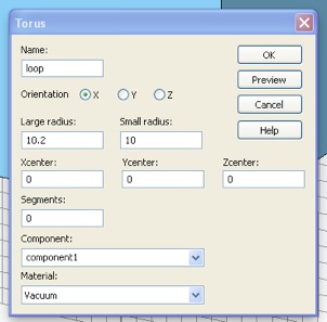
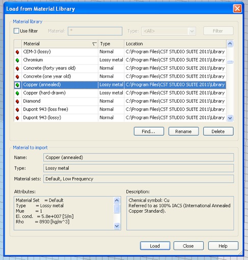
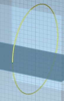
Now make a loop. Select the Torus creation tool (i.e. the small doughnut icon). Select X for the Orientation, so that the plane-wave magnetic field will thread the loop. Make the inner (small) radius 10 mm and make the outer (large) radius 10.2 mm, so that the loop wire diameter will be 200 μm. Next, select [Load from Material Library...] from the Material menu.
This will bring up the Material Library panel. Find and select “Copper (annealed)” from the list. Click Load. Then click OK in the Torus panel.
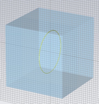
Your torus should look like this.
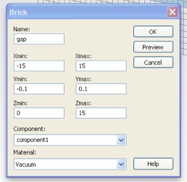
We want a gap in the ring so we can insert a load with which to monitor voltage and current. Make a slab of Vacuum to insert into the ring. Make the gap 200 μm. (I made the slab 30mm wide and 15mm deep, but that is somewhat arbitrary.)
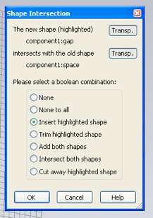
This new shape intersects with both the existing shapes you have made. CST wants to know how to handle this since every point in the simulation domain must have one, and only one, material specification. For both Shape Intersections choose “Insert highlighted shape”, and click OK.
Your split loop should look like this.
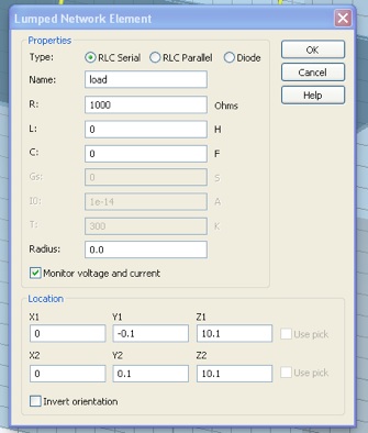
Select Lumped Elements... from the Solve menu. Set the lumped parameters for a 1KΩ resistor. Enter the Location as below, so that the lumped element will be centered and span the loop gap. Also, check the “Monitor voltage and current” box.
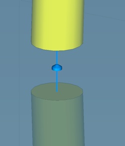
If you zoom in, you can see that the lumped element sits in the center of, and spans, the gap.
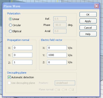
Select “New Plane Wave...” from the Solve Menu. Change the Electric field vector from x-polarized to y-polarized (compatible with the boundary conditions we selected) and with a magnitude of 1000 V/m.
If you select the Plane Wave in the Plane Wave folder of the Navigation Tree you will see a graphical representation of the plane wave at the boundary of the simulation domain, including the orientation of the fields. You can see that the magnetic field will thread the loop and induce a potential there in. This plane wave will launch from that surface and propagate through the entire volume of the simulation domain.
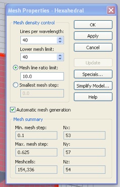
Since the loop wire is thin, we should increase the mesh density. Select Global Mesh Parameters... from the Mesh menu. Set the Mesh density control parameters, “Lines per wavelength” and “Lower mesh limit”, both to 40.
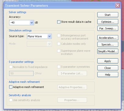
Finally, open the Transient Solver panel, from the Solve menu (or with the red, “T” icon). Set the Accuracy to -40dB and click “Start”.
The solver will take about five minutes. You can ignore the warning message about “staircase mode”. When complete, select the “Lumped Elements >> Voltages >> |U| linear” folder in the Navigation Tree. Here you can see how the potential magnitude at the load varies with frequency.
Develop an expression for the load potential magnitude, in terms of the loop radius, a, electric field magnitude, E, frequency, f, and the speed of light, c. Note that for a plane wave the magnitude of B is E/c.
What is the functional form of the dependence on frequency? Does the shape of the plot from simulation agree with this?
Compare the value of your expression with the value from the plot at 100 MHz. If you right click on the plot and select “Show Axis Marker”, you can extract precise values. Report the fractional difference. (Be careful with units.)
Optional: suggest a reason why the curve diverges from the Faraday result at higher frequency. (Hint: inductor self-resonance.)