Project 2
Project 2
We will simulate something vaguely resembling an iPhone 4 antenna and determine its properties with and without a finger on the, so called, “death spot”.
First construct a model that captures the basic configuration of the handset’s antenna. It is possible that (as this person believes) the antennas are essentially slot antennas as outlined in an Apple patent.
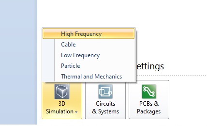
As before start a High Frequency, 3D Simulation
Set up the same units as last time (mm, GHz, nS). Set the frequency range to 0 to 2 GHz. Set the Background Properties to Normal with Epsilon = Mue = 1.
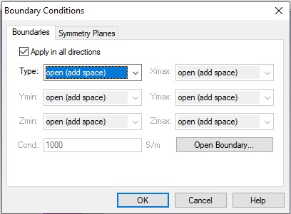
Set the Boundary Conditions all to open (add space).
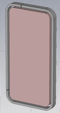
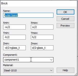
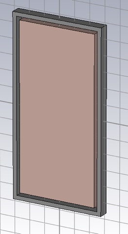
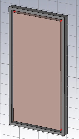
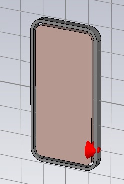
The innards (between the glass front and back) can be modeled as a single brick of metal. The outer-most part will be a steel band circumscribing the handset with two splits to create slot antenna boundaries. Use Copper (annealed) (lossy) for the innards and Steel-1010 (lossy) for the outer band, though obviously these are rough approximations. Use global parameters for all the geometric properties so we will have ample tuning capability. When the metal parts are done, it will look like this.
Start by making a slab of the steel
When you use symbols for numerical fields, CST creates a global parameter for you and asks for the initial value. We will use all global parameters with the following initial values:
For initial values use:
exterior corner radius = 10mm
exterior dimensions use Wikipedia specs
metal thickness = 6.3 mm
glass thickness = 1.5 mm
outer band width = 2.5 mm
slot width = 2 mm
left lower slit position, below center = 43 mm
left upper slit position, left of center = 10 mm
split width = 1 mm
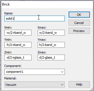
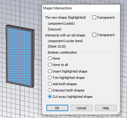
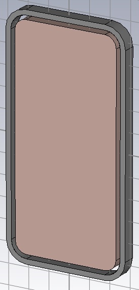
Now we want to cut away the interior. Create a slab of Vacuum to define the cut out region.
CST wants to know how to handle the overlapping regions. Choose Cut away highlighted shape.
Now create the interior copper slab. You can change the copper to a copper color by double clicking the material in the Materials folder of the Navigation Tree.
Now we want to blend the edges. First select the edges of the copper slab. Press the ‘e’ key and then double click the desired edge. Repeat for the other three edges. You will need to rotate and zoom to get a clear shot at selecting the all the edges.
Choose Blend edges...
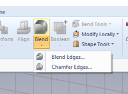
Enter the correct radius. You want all the corner radii to have the same center of curvature. Blend all the other corners.
Create the two slits by creating a thin slab to cut away the band. The upper slit cut away is shown below.
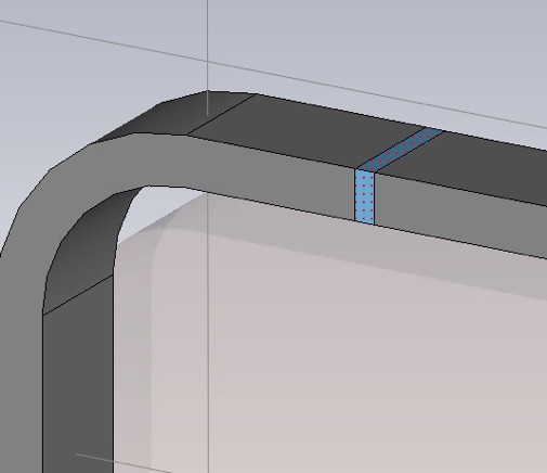
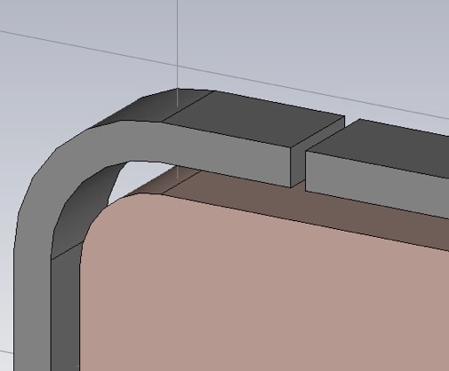
Create the lower slit.
Now add the glass to the front and back. Use Glass (Pyrex) (lossy) because we do not have a model for the fancy aluminosilcate glass that Mr. Jobs specified.
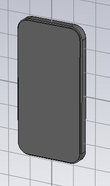
Set the glass back from the edge as on the real handset. For an initial value of the set back use 1 mm, and again, use blending radii such that all blends have the same center of curvature. You can use Transform to duplicate one sheet of glass to make both front and back. I will explain this in class. I chose to change the color the glass to make it look more iPhone like.
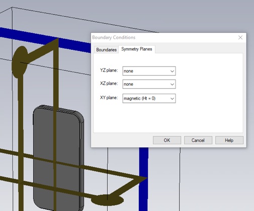
Since our model of the handset is mirror symmetric, front-to-back, you can add one symmetry plane, for a 2X speed-up. Electric or magnetic? This symmetry plane must be compatible with the fields generated by the discrete port. Another way to think about it is to consider what would happen if you put zero impedance surface or a zero admittance surface at the proposed location. Symmetry planes are set in the Boundary Conditions panel.
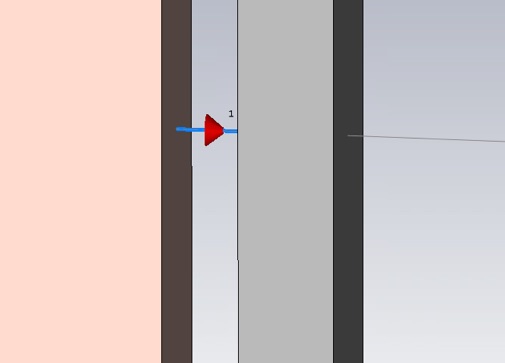
Now add a discrete port that will function as an antenna feed. Use the default 50 Ohms for the impedance (a guess). The Discrete Edge Port panel is accessible from the Simulation Tab.
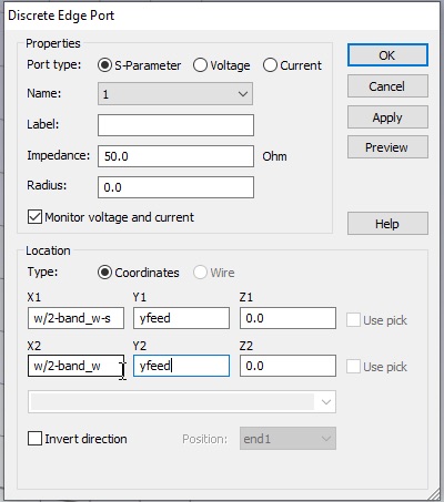
When selected the port is shown as a blue line with a red cone indicating the polarity. It should span the slot, and should probably lie in the center (front to back) of the slot. For the initial value of the vertical posiiton of the feed, choose 40mm below the center. You probably want to zoom in and hide the glass to confirm the port is where it ought to be.
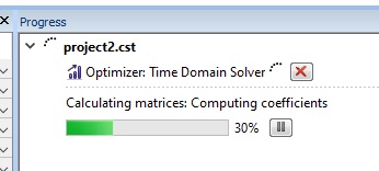
Now we can simulate. We will use the optimizer to find locations of the splits and feed that will maximize the antenna efficiency. For the purpose of seeing the optimizer progress in a reasonable amount of time, we will prioritize speed over accuracy. Open the Time Domain Solver Parameters panel. Leave the accuracy at -40dB. Under Specials.... Under the Steady State tab increase the Number of pulses to a bigger number like 200, and under the General tab, give the frequency samples a modest boost to 4001 from 1001.
Now start the simulation. Confirm that the simulation takes about 30 seconds or less. Then look at S11. We will target the center of the LTE band 3 uplink.
https://en.wikipedia.org/wiki/LTE_frequency_bands
Do we have an S11 dip in this band?
Now select Optimizer...
In the Parameter table select the variables controlling the locations of the feed and the splits, and give them the biggest range that keeps the splits and feed on the straight portion of the steel outer band. Select one of the global optimization algorithms. I used the Genetic Algorithm.
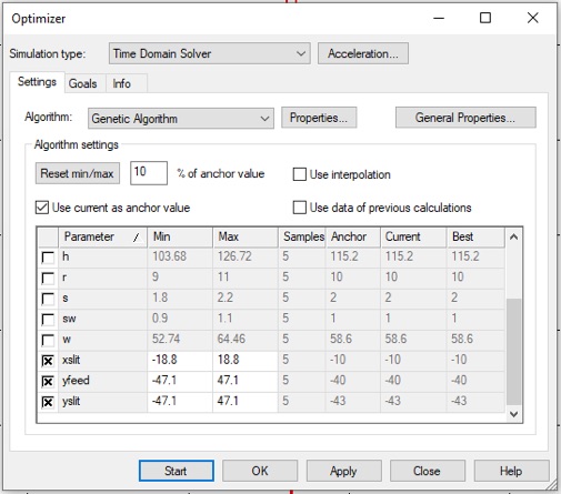
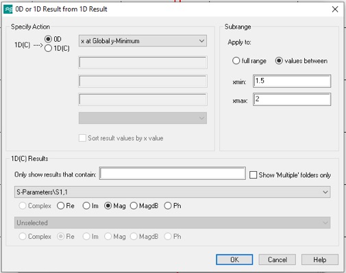
Select the Goals... tab, then Add New Goal..., and Result Template.... In the top menu select General 1D in the top menu and 0D or 1D Result from 1D Result in the bottom menu. In the next panel’s menu select x at Global y-Minimum, and S1,1mag for the 1D result to be used. Then use a subrange of 1.5 to 2.
Click OK.
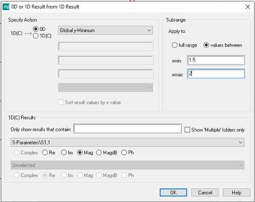
Select 1D Result from 1D Result in the bottom menu again. This time pick Global y-Minimum. Use the same subrange.
Click OK. Then close the Template Based Postprocessing panel.
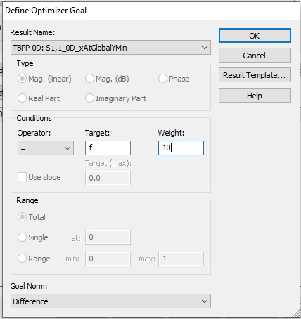
In the Define Optimizer Goal panel, select xAtGlobalYMin, and use the = operator, a variable for the Target, and 10 for the weight.
Click OK. Set the target frequency as mentioned above.
Add another goal for GlobalyMin.
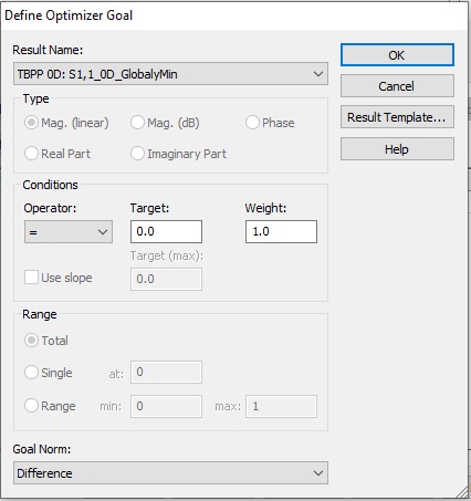
Your two goals should look like this
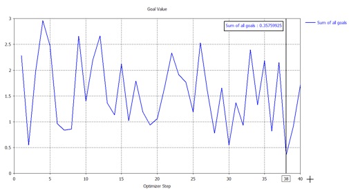
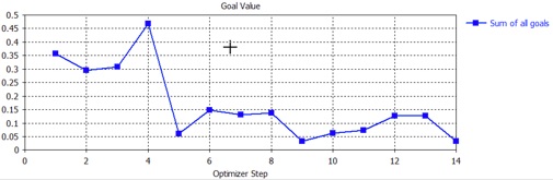
Now click Start to begin the optimization. Each sim should take about 15 to 60 seconds. Let it run until you get a Sum of all goals less than 0.5
1. Save a screen capture of the Sum of all goals plot, with an axis marker at the minimum. (The axis marker can be automatically moved to the minimum.)
Now, click the red X in the progress window to abort.
...and then choose Reload best results.
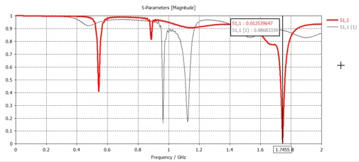
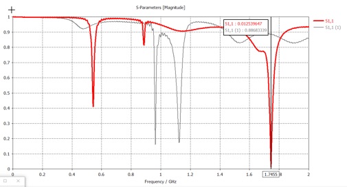
2. Get a screen capture of an S11 plot, with an axis marker at the minimum.
Now go back to the Optimizer panel. Switch from a global algorithm to a local algorithm, like Trust Region Framework. Make sure the Use current as initial value box is checked, so that the local optimization will start where the global optimization left off.
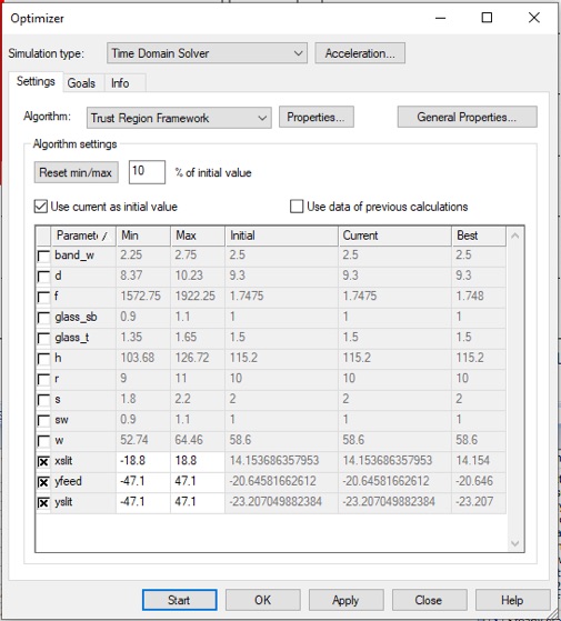
Click Start and let the optimization run to completion.
-
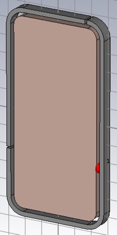
3.Get screen captures of the Sum of all goals and S11 plots as before. How much did the S11 dip (frequency and depth) improve by using the local optimization after the global optimization. Also Provide a picture of the phone in the optimal configuration (with the glass hidden), and report the numerical positions of the splits and feed with respect to the handset center..
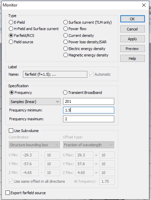
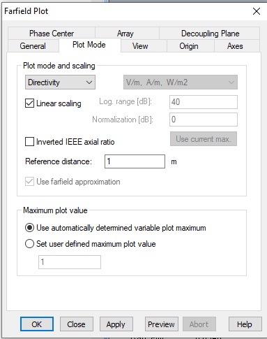
Make a field monitor, so we can view the farfield radiation and also find the power distribution and efficiency. Click the Field Monitor button on the Simulation tab. Choose Farfield/RCS and set the Frequency parameters as shown.
Re-simulate using a higher accuracy of -60dB. Since we will run just one simulation at time from this point on, we can wait a bit longer for higher accuracy. This higher accuracy will make the curves smoother with less truncation artifact.
4. Get a power plot by selecting 1D Results>>Power>>Excitation [1]. Adjust the frequency axis to display 1.5 - 2 GHz, and put the axis marker at your targeted frequency. For most of you that will be 1.7475 GHz, but if you chose another nearby frequency, that is OK, stick with your targeted frequency.
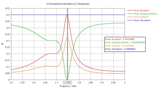
5. For this optimal configuration, report the fractional power distribution of the stimulated power, specifically report the fractional power: reflected, radiated and absorbed, at the target freqeuncy. The absorbed power is whatever is left over from reflection and radiation, and will include power absorbed in the copper, steel, and glass.

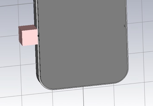
Now let us try to simulate the iPhone 4 death grip. Put a cubic centimeter of skin material centered on, and touching, the left-side split. Re-simulate.
6. Report the power distribution as in question 5. What is the drop in radiated power (in dB) induced by touching the split? Where is most of the power going, that is now not being radiated? Did the absorbed power go up or down? Why? Would you say that the antenna performance has been reduced or shifted?
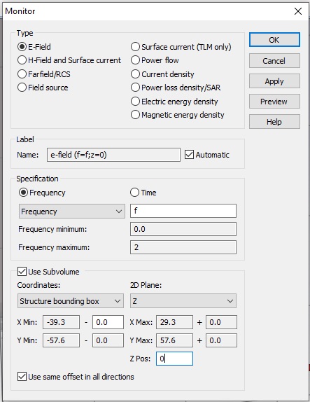
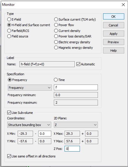
Let’s add some local field monitors for both E and H. In particular, we want to look at our operating frequency and in the plane of the slot.
Make sure your farfield monitor is still present, and run one last simulation at the optimal configuration, without the finger. You can hide the commands the created the finger in the History List.
7. Include the following E and H plots of the slot fields in your report. Select from the navigation tree: 2D/3D Results>>E-field>>e-field (f=f,z=0)>>Abs. Adjust the Min and Max values to best display the field minima and maxima of the fields in the slot.
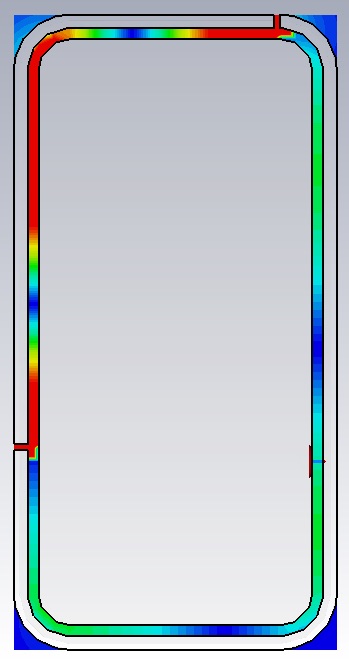
Do the same for the H-field.
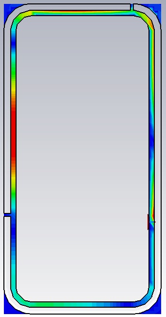
Consider the magnitude of both E and H, and identify positions of maximum and minimum characteristic impedance of the slot waveguide. Mark these locations on either your E or H plot (or both), with a ‘+’ and ‘-’ for maxima and minima respectively. Is the feed point closer to an impedance minima or maxima? What is the approximate impedance at the location of the feed? Is the impedance a maximum or minimum at the splits? What does this suggest is the termination condition of the slot waveguide at the splits.?
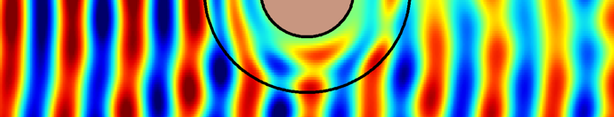
8. Include a far-field plot in your report. Select from the navigation tree: Farfields>>farfield (f=1.7475). From the Farfield Plot Properties, make the phone appear together with the radiation pattern. Include a couple views that communicate most of the pattern geometry.
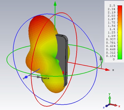
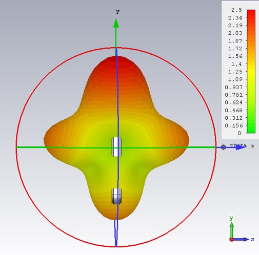
Describe two qualitative differences in the radiation pattern between this antenna and a dipole antenna. How does this antenna’s directivity compare to that of a half-wave dipole antenna?
How does the longest dimension of this phone compare to the length of a half-wave dipole at our operating frequency?