|
1
|
|
|
2
|
|
|
3
|
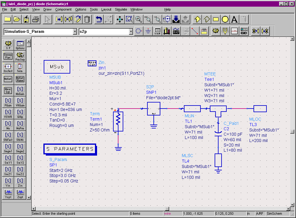
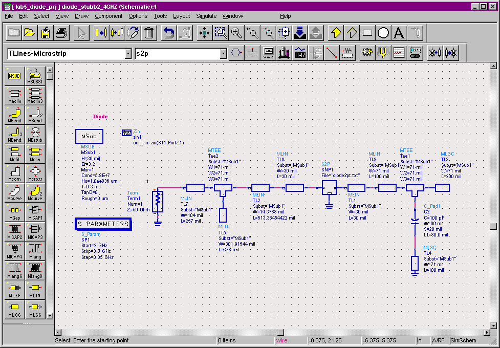
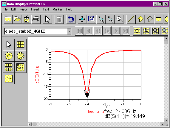
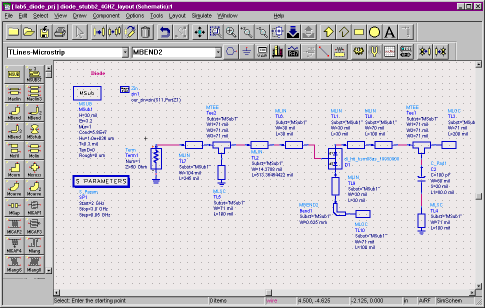
- Use this part of the tutorial to simulate the RF performance of your
circuit. You need to include the
lengths of all lines (including the pads for soldering elements
to). These are found in the
layout section, so you will do some back-and-forth between layout and
simulation.
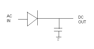
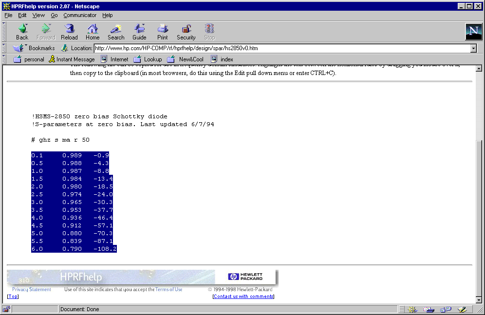
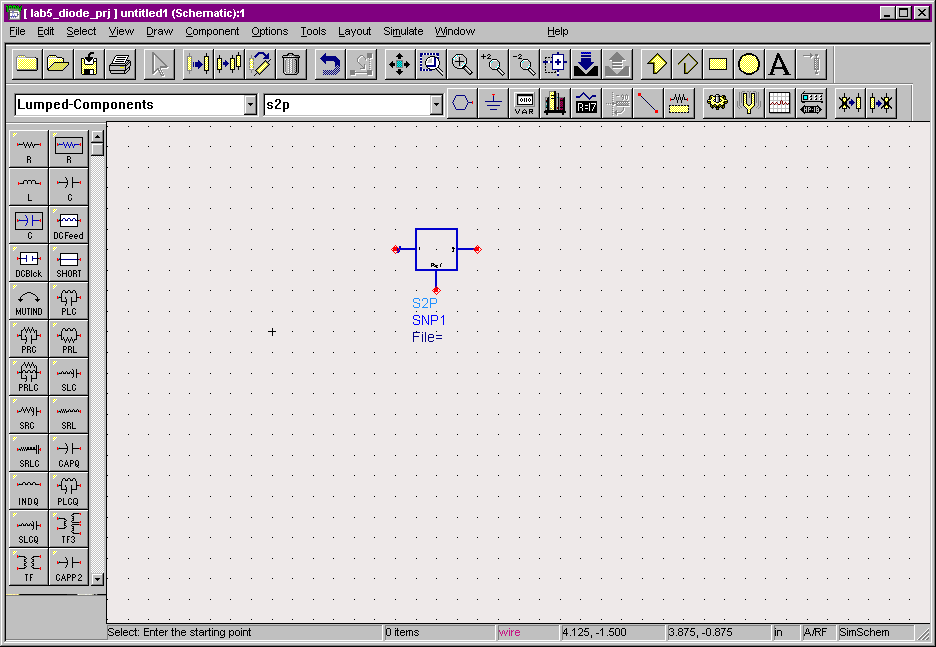
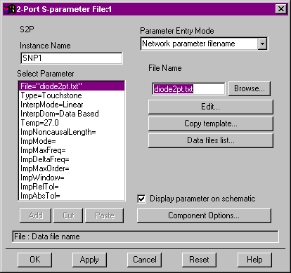
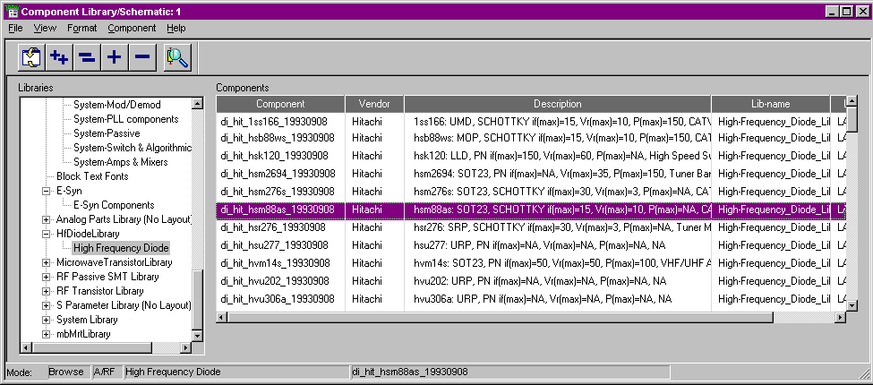
- Some elements are available in the standard libraries (the cap in this
lab), others are not (the diode in this lab). When they are not available, you will
have to “create” them using user-defined S-parameters and lines
(MLIN). These can come from data
sheets (like the HP website) or from measurements (like for this lab).
|
|
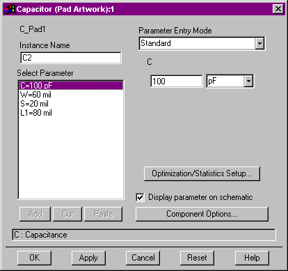
4
|
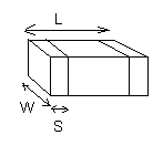
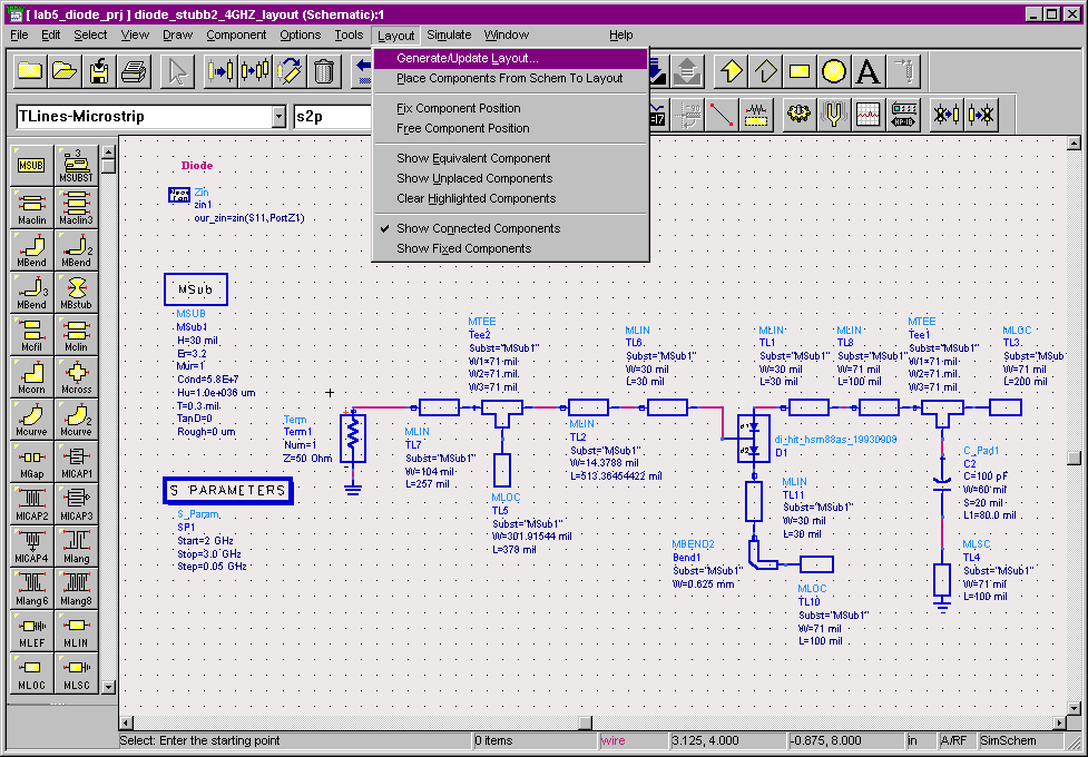
- “Artwork” is used to define the size and shape of solder connects for
components like capacitors, diodes, RF chips, etc.
- The dimensions of solder pads (where you actually connect your circuit)
are specified on data sheets.
They are also available in the libra “library” for many standard
elements.
- The size of pads add length to your lines, so you will need to include
them in your simulation for most accurate results. This means you need to figure out
their size before you simulate the circuit, so you will do some
back-and-forth between layout and simulation.
|
|
5
|
- Measure them (most accurate)
- Find them on the web or other data sheet (we’d like this to be most
accurate, but for this lab it isn’t)
- These methods are described below, for your reference. Measured values are given at the end.
|
|
6
|
- Build the circuit with just a length of line attached to the device.
- Measure the input impedance using the network analyzer.
- Compensate for the length of the line to find the S-parameters of your
device (Matlab code to do this is included)
|
|
7
|
|
|
8
|
|
|
9
|
|
|
10
|
|
|
11
|
|
|
12
|
|
|
13
|
|
|
14
|
|
|
15
|
|
|
16
|
|
|
17
|
|
|
18
|
|
|
19
|
|
|
20
|
|
|
21
|
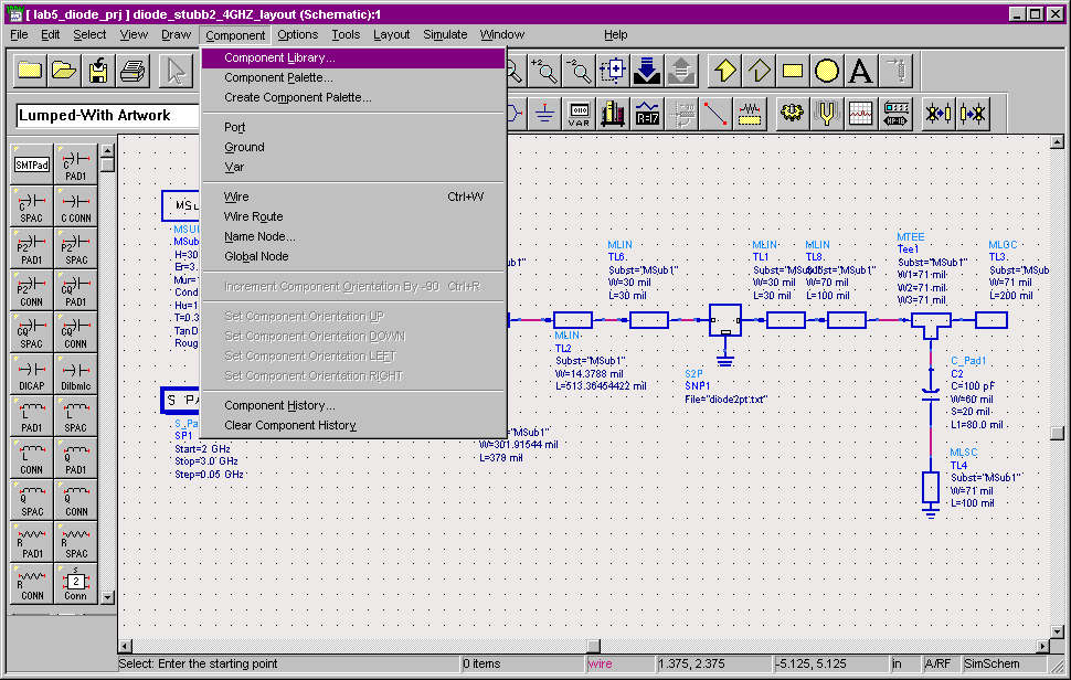
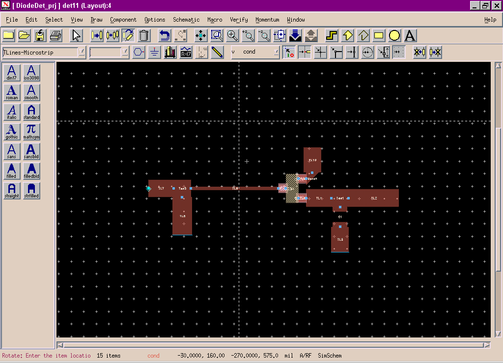
- You have now simulated how your circuit should work, but you can’t mill
it. The mill will not know what
to do with the S2P element and won’t leave any particular solder pads
for the capacitor.
- In this part of the tutorial, you will prepare the circuit to be
soldered, but won’t be able to simulate its performance.
|
|
22
|
- “Artwork” is used to define the size and shape of solder connects for
components like capacitors, diodes, RF chips, etc.
- The dimensions of solder pads (where you actually connect your circuit)
are specified on data sheets.
They are also available in the ADS “library” for many standard
elements.
- The size of pads add length to your lines, so you will need to include
them in your simulation for most accurate results. This means you need to figure out
their size before you simulate the circuit, so you will do some
back-and-forth between layout and simulation.
|
|
23
|
|
|
24
|
|
|
25
|
|
|
26
|
|
|
27
|
|
|
28
|
|
|
29
|
- Remove all parts that will be soldered on (diode and capacitor) before
saving the file to be milled.
- If you don’t, it will “mill” their outline and mess up your board.
|
|
30
|
|
|
31
|
- Design two diode detectors, one for 2.4 GHz, and the other for 2.4
GHz. (Slight change in single
stub match.)
- Print out the layout of your diode detectors, with sizes clearly marked.
- Clearly mark where holes for shorts should go (there will be two on each
detector).
|
|
32
|
- If you didn’t “get” something in this tutorial, please tell Dr. Furse or
You Chung which slide(s) is confusing.
- Thank you!
|

 Notes
Notes